| Molecular Formula | GaAs |
| Molecular Weight | 144.64 g/mol |
| Crystal Structure | Cubic |
| Color | Metallic dark gray |
| Odor | Garlicky when moist |
| Melting Point | 1238 °C |
| Solubility | <1 mg/mL at 20 °C |
| Density | 5.3176 at 25 °C |
Structure
Gallium arsenide (GaAs) consists of larger arsenic atoms (violet) connected to somewhat smaller gallium atoms (salmon pink). Each arsenic atom allows four gallium atoms to covalently attach to it, but those gallium atoms can attach with two other arsenic atoms. This allows the GaAs to have an indefinite molecular size as this pattern repeats, forming what is called a network covalent crystal.
We only consider a single portion of the entire complex called the unit cell, shown in Figure 1. It takes the form of a cubic structure. This unit cell can be placed and attached side by side with other unit cells to complete the crystal.

Source: https://en.wikipedia.org/wiki/Gallium_arsenide#/media/File:Gallium-arsenide-unit-cell-3D-balls.png
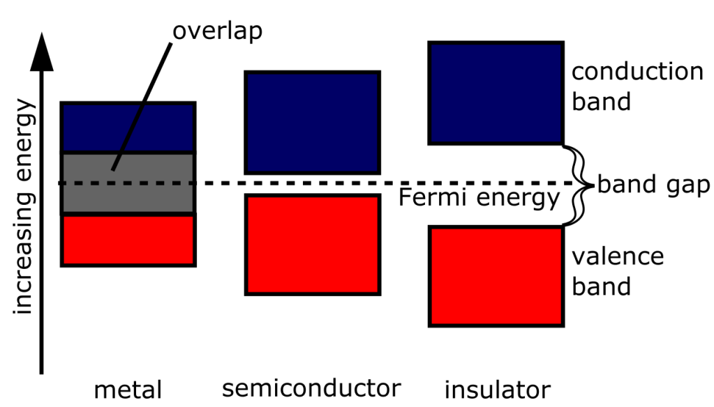
Now, every material varies by its conductivity. Conductivity is determined by how much energy is needed to promote the electron from its bound state to the atoms, called the valence band, to the level in which it can freely move, called the conduction band. The lower the amount of energy is needed to promote the electron – that is, the smaller the “band gap” – the more conductive it is. Conductors thus have a narrow to non-existent band gap, semiconductors are thus characterized by a small band gap, insulators by a large band gap.
Synthesis
The most common way of preparing GaAs is through the Birdgman-Stockbarger method. In that method, a crucible containing the polycrystalline material (in this case GaAs) is placed in a tubular furnace where it is heated and made molten. However, down that furnace, there is a temperature gradient – meaning to say, the amount of heat per position inside the tubular furnace varies. In the Bridgman-Stockbarger method, the furnace’s temperature decreases downwards vertically. Thus, the lower regions of the crucible are cooler.
A seed crystal that follows a specific crystal structure is placed at the lowest portion of the crucible. As the crucible is lowered then, the molten gallium and arsenide is cooled and eventually solidifies around the seed, following its structural pattern.
Trivia and Uses
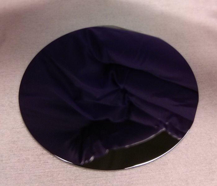
Source: https://commons.wikimedia.org/wiki/File:Gallium_Arsenide_(GaAs)_2%22_wafer.jpg
GaAs has become somewhat of a standard material in experimental physics and engineering. Crystals of GaAs also a neat property in which the jiggling of its electrons in the valence band are in sync with the electrons in the conduction band. This property allows it to emit (and absorb) photons with high efficiency.
This makes GaAs useful in constructing near-infrared emitting diodes, which emit photons, and solar cells, which absorb them.
GaAs can also be used as a semiconductor in transistors found in computers, but its low thermal conductivity and high tendency to expand due to heat make it complicated to use. Its low manufacturing cost, however, makes up for such complications.
References
Alineason [Internet]. c2020. Frankfurt, HE: Alineason Materials | Technology [cited 2020 July 16]. Available from: https://www.alineason.com/en/knowhow/crystal-growth/.
Azom [Internet]. c2013. Sydney, NSW: AZo Materials [cited 2020 July 16]. Available from: https://www.azom.com/article.aspx?ArticleID=8349#:~:text=The%20applications%20of%20gallium%20arsenide,laser%20diodes%20and%20optical%20windows.
PubChem [Internet]. c2020. Bethesda, MD: National Center for Biotechnology Information [cited 2020 July 16]. Available from: https://pubchem.ncbi.nlm.nih.gov/compound/Gallium-arsenide#section=Information-Sources

_2%22_wafer.jpg)